Applied and Integrated Photonics
- Compact optical tweezers system with MEMS steering optics and optomechanics for biomedical applications.
- The use of photolithographic methods, wet and dry etching to produce optical elements, microfluidics and metasurfaces.
- Microchip for optical trapping of micro-objects under low pressure.
- Metaoptics structures for aberration-free imaging and spectroscopy systems.
- Inspection by Scanning Probe Microscopy with emphasis on the surface topography of prepared nanostructures and films & coatings.
- Determination of mechanical properties such as elastic modulus, hardness or film adhesion by nanoindentation measurements and scratch testing.
- Microfluidic acoustic wave based sorting chips.
- Arbitrary shaped optical gratings and micro-optical elements.
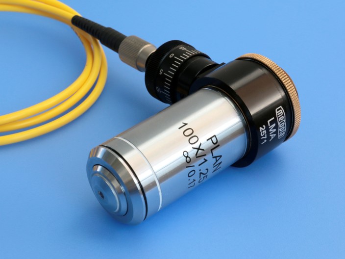
Compact device for creating optical tweezers attachable to a Raman microscope.
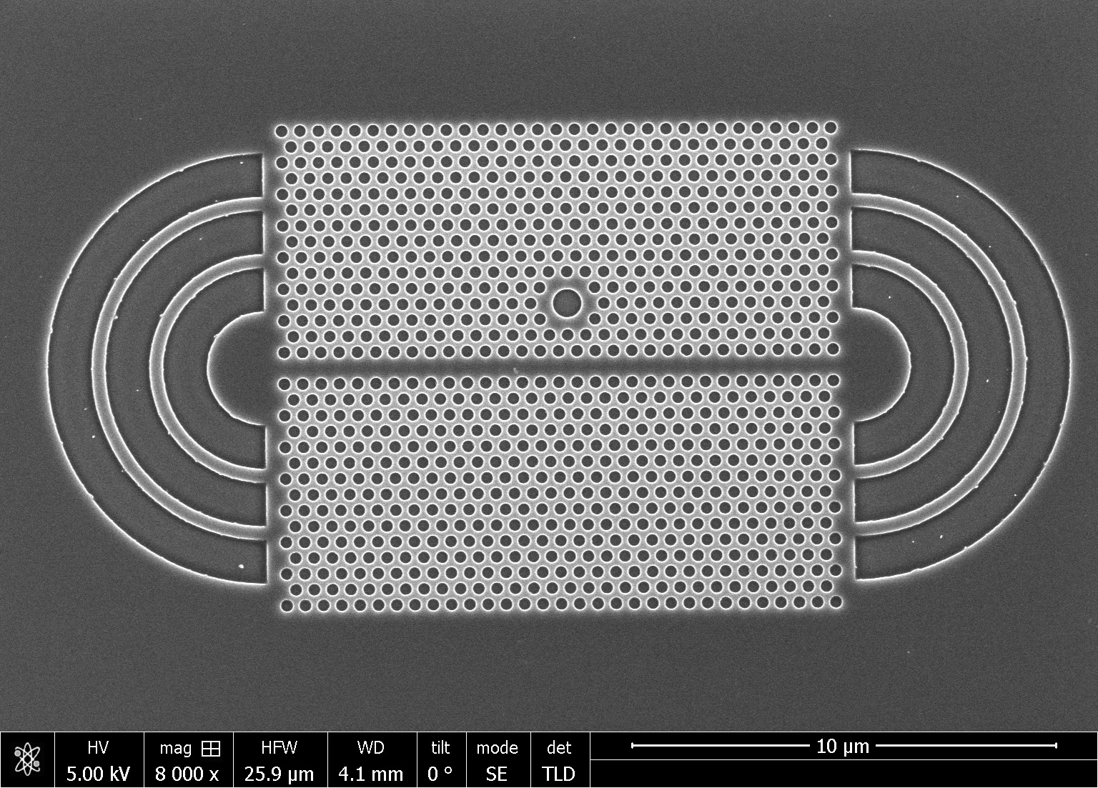
Photonic element designed to trap particles (SEM image).
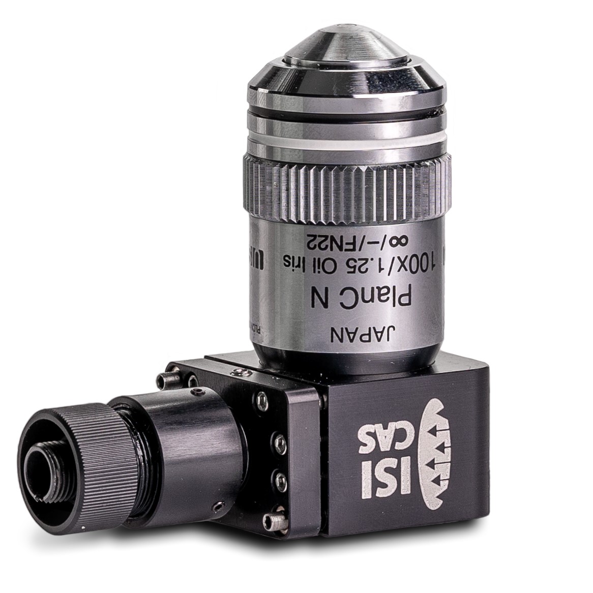
Compact optical tweezers module can be attached to any kind of optical microscope.
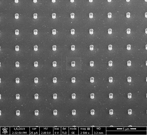
Sub-micrometer columns, prepared into silicon by reactive ion etching.